
TECHNOLOGY NEWS
Substrate Integrated Circuits (SiCs) – A Paradigm for Future Ghz and Thz Electronic and Photonic Systems
1. Introduction
High-frequency integrated circuits (ICs) are the fundamental building blocks and “life” elements for radio-frequency (RF), microwave and wireless electronics and photonics, which are essentially made of planar conducting traces and lines on dielectric substrates or layers through various processing techniques in conjunction with semiconductor devices (diodes/transistors). The basic features of high-frequency ICs with respect to their low-frequency counterparts are that high-frequency structures require low-loss dielectric substrate with appropriate line width and specific substrate thickness without further mentioning much more involved circuit pattern design and termination conditions. The most well-known technique of ICs fabrication is probably the low-cost printed circuits board (PCB), which can be used to construct two-dimensional (2-D) single-layered and three-dimensional (3-D) multi-layered structures. Generally speaking, such circuits become carrier circuit boards, thus allowing the integration (usually surface-mounting) of lumped- and/or distributed-element passive components and active devices into the same platform. More sophisticated high-density and large-scale circuit integration can be made with CMOS and monolithic microwave integrated circuits (MMICs) in which passive and active circuits are completely made and integrated within the same semiconductor substrate. Today’s advanced techniques even allow the integration and combination of MEMS, LTCC and other circuits and antennas with CMOS and MMICs in various topological and packaging forms such as system-on-package (SoP) and system-in-package (SiP).
Unfortunately, such well-established circuits and systems design platforms would experience increasingly performance-related degradations as operating frequency (analog) and speed (digital) become higher and higher, well going into GHz range for now and even extending into THz domain in the near future. In addition to the widespread use of lumped-element approaches well-known for their frequency limitations, the fundamental problem in the design is closely related to the performance-sensitive planar transmission line structures at higher frequencies including microstrip lines, coplanar waveguide (CPW), and their various structural derivatives [1-2]. It is known that the planar lines suffer from high conductor loss because of the singularity of current density distributions over their line edges [3-4]. Additional conductor losses caused by the ground planes may be more pronounced in thinner substrate layers, which are usually the case of 3-D stacked semiconductor or other micro-fabrication-based structures. In addition, planar structures are somewhat unbounded at least in geometry and they are naturally subject to leakage loss, radiation loss, mode conversion loss, and line-to-line cross-coupling problem. Those adverse factors create huge and difficult-to-solve problems in various practical designs and application scenarios, namely, high-density integration, high-frequency operation, integrated system packaging and circuit interconnects. It can be postulated that the high loss effect and frequency-sensitive coupling severely handicap the circuit operation at frequencies beyond 60 GHz if low-cost conventional processing techniques are used.
Interestingly, the predecessors of planar structures such as rectangular waveguide and coaxial line that were developed during and after World War II have not been completely replaced by them. In fact, such non-planar structures have been still continuing to play critical roles in many of our today’s GHz circuits and systems. This is because those “old” technologies exhibit uneven electrical and mechanical performances compared with their planar counterparts such as transmission loss and power handling capability. However, such “old” technologies cannot be used for circuit and system integration because of their bulky mechanical and non-planar nature, and also they are rather tolerance-sensitive [5-6]. This bottleneck problem becomes much more pronounced at higher frequencies such as millimeter-wave range.
On one hand, there are many problems in the design of high-performance planar highly integrated circuits with the current microstrip and CPW structures. On the other hand, it is impossible to develop any integration platform with the conventional non-planar waveguide techniques. Obviously, there is a fundamental gap between the planar and non-planar structures judging from circuit performance, integration issue, and even cost aspect. With any state-of-the art techniques, it is impossible for us to find an outstanding compromise between the two classes of structures unless we can technologically “merge” them into the same family. This begun with the invention and development of substrate integrated circuits or SICs [7-10].
This technology news report briefly describes this emerging high-frequency technology, which may revolutionalize our current and future design and development of GHz and THz integrated electronic and photonic circuits and systems. Note that the following sections have excerpted some paragraphs from the author’s invited presentation at the JNM 2009 (Journees Nationales Microondes 2009) – Grenoble, France.
2. Substrate Integrated Waveguiding Structures
To fundamentally merge the above-discussed two different classes of planar and non-planar structures into the same design and fabrication platforms, we have proposed and developed the concept of substrate integration that allows the “planarization” of non-planar structures such as rectangular waveguides, coaxial lines, and dielectric waveguides, and etc. In this way, the non-planar structures can be made in planar form and they can completely be integrated together with planar structures onto the same planar substrate with the same processing or fabrication techniques.
In this way, the non-planar structures become united with the conventional planar structures. Theoretically, any non-planar structure can be made in planar form with certain modification of geometry, which should preserve however the basic features of the original non-planar structures in terms of guided-wave characteristics and other structural properties. Note that the realization or synthesis of such a “non-planar structure” in planar form depends on a series of factors, in particular, enabling fabrication or processing techniques.
Figure 1 describes a family of substrate integrated waveguiding structures that are not complete in this report (only three typical structures are shown). Among them, the substrate integrated waveguide or SIW has been the most popular because of its easy fabrication and similar electrical and mechanical performances with respect to the conventional rectangular waveguide. Therefore, it has been well exploited and demonstrated for various microwave and millimeter-wave applications ranging from few GHz to few hundreds GHz [11-21, for example].
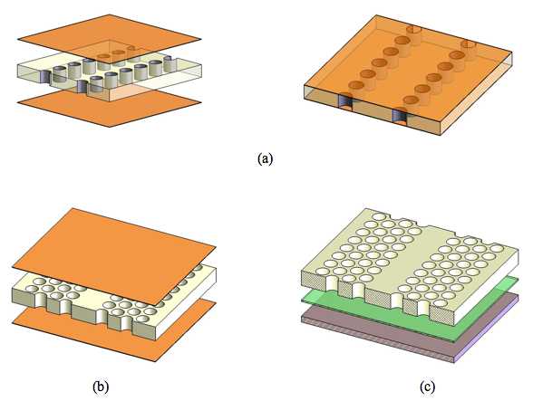
Figure 1 (right):Typical examples of synthesized substrate integrated waveguiding structures compared to their original non-planar versions: (a) substrate integrated waveguide (SIW); (b) substrate integrated non-radiative dielectric (SINRD) guide; (c) substrate integrated image guide (SIIG).
The SIW is synthesized through the use of arrays of metallized via hole or slot trench, and this technique can directly be applied to some other non-planar structures. Those artificial arrays create equivalent “electrical” fences or walls into which electromagnetic waves or fields are confined. With a relatively thin thickness of dielectric substrate, the synthesized planar structure is found to have a much broader monomode bandwidth compared to its rectangular non-planar counterpart. In addition, the power handling capability [22] and loss performances of the SIW are much better than the conventional planar lines. This makes the SIW circuits and systems attractive for practical applications. On the other hand, some other non-planar structures such as dielectric waveguides can be synthesized into planar counterparts through the use of air hole/slot arrays. In this case, the air hole/slot arrays are used to reduce the equivalent dielectric permittivity in the region of interest so that the equivalent waveguiding channel is created through the contrast in dielectric constant or index. This is very similar to the making of optical waveguides. However, this is different from the photonic bandgap structures [23-24].
Naturally, a synthesized planar waveguide as shown in the above figure may have a higher loss than its original version because of the filled-in dielectric material. Such a periodic structure is always subject to bandgap-related (or stopband) dispersion behavior, which occurs at much higher frequencies than its operating band. This problem may present interesting opportunities since we can use special dielectrics and other material effects to realize some functionality such as size miniaturization, electronically and/or optically tunable capability, electro-optical and acoustic design, and others. In particular, with the advancement of nano-structured materials and the exploration of smart materials, we can anticipate many novel devices and circuits coming out of this substrate integration technique. Probably, we would have room-temperature-based extremely low loss or even “zero” loss (loss tangent small than 10-6) dielectric materials in a not-so-distant future. This will be a certainly technical revolution in the world (a true Nobel Prize event).
Usually, substrate integrated structures are frequency-sensitive except the substrate integrated coaxial lines that support TEM mode. Therefore, the design and realization of a structure are closely related to a specific processing technology and its frequency range of interest. Current high-precision PCB techniques including LTCC process should enable us to design the SIW structures up to 100 GHz while advanced micro-fabrication techniques such as photoimageable, micromachining, CMOS process, and others would easily allow the design of substrate integrated structures up to hundreds GHz and THz range. With the substrate integrated dielectric waveguide techniques, the operation should be able to cover the whole THz range. This suggests that the proposed substrate integrated waveguiding structures provide a fundamental integrated guided-wave solution to the development of THz integrated circuits. In addition, there are three interesting outlooks anticipating this development: (1) dielectric contrast can also be made with high-index material doping and diffusion; (2) various waveguide topologies can be mixed together within the same planar substrate; (3) special guided-wave phenomena may be explored such as Plasmon and left-handed material. Generally speaking, metallic waveguide is more relevant to electronics while dielectric waveguide is more prone to photonics. Therefore, the SICs could effectively bridge the two different worlds, namely, electronics and photonics.
In addition, the electrical size of those synthesized waveguides can be elastically manipulated through the choice of dielectric materials and other techniques (electronically-controlled ferroelectric substrate, e.g.). This provides a special means in developing miniaturized waveguide structures. In addition, the thin substrate allows the “slicing” of those planar substrates without much perturbing the operating modes [25-27].
3. Substrate Integrated Circuits
3.1 Substrate integrated transitions
The conventional planar lines are still required today for active device design and integration even though they may be removed in the future if solutions to integrating active elements directly into the “synthesized planar waveguides”. To enable a seamless integration between those two dissimilar classes of structures on the same substrate and/or in multilayered substrate, high-quality transitions are extremely critical to ensure low-loss, broadband and compact size structures. In addition, transitions are also required for connecting different synthesized planar waveguides in the same platform, which will not be discussed here for brevity.
Presently, a number of broadband and low-loss transitions have been proposed for practical applications [9, 28-31], which have been used in the design of various SICs that will be discussed briefly in the following sections. It is important that simultaneous field and impedance matching schemes should be considered because the modes in those dissimilar structures are different as shown in Figure 2. This can clearly be observed in a multilayered structure [30]. Essentially, various transitions between CPW and SIW and between microstrip line and SIW are of particular interest to the current SIW-based integrated circuits. In [29], an interesting mode conversion can be made mutually between two dissimilar structures within the same structure platform. This scheme would be very useful for designing in-line coupler and distributed devices such as traveling-wave amplifiers and antennas. Figure 2b and Figure 2c show the structure of such a mode conversion mechanism and its theoretical and experimental results (detailed information on the choice of parameters can be found in [29]). Multilayered transition techniques can also be made for high-density circuit design [30].
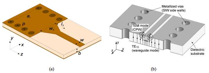
Figure 2 (left): Broadband transitions of two dissimilar structures: (a) SIW-microstrip transition, and (b) SIW-CPW hybrid mode lines
Recently, a very low-loss broadband CPW-SIW transition having ultra-short length has been proposed and demonstrated in [31], which is very important to the design of low-loss or high-Q integrated SIW structures and circuits. This is because the choice of thicker substrate allows the reduction of conductor losses. However, this is not easy for the co-design of SIW and microstrip line circuits because the characteristics of microstrip line are very sensitive to the dielectric thickness such as characteristic impedance. Furthermore, the choice of characteristic impedance for the microstrip is quite limited, which is not practical for its active device integration. Therefore, the CPW presents an ideal platform but its transition bandwidth was relatively narrow. With the new advancement, it can be expected that we will be able to design flexible and high-quality CPW-SIW SICs.
3.2 Substrate integrated circuits and antennas
Various passive and active SICs have been proposed and demonstrated since about eight years of the development of SICs concept, which include couplers, resonators, filters, diplexers, circulators, oscillators, amplifiers, oscillators, and mixers. Those circuits have been designed and measured over a very wide frequency range from 5 GHz to 250 GHz. Most of those SICs are realized on single layer low-loss dielectric substrate. It can be claimed that all of those front-end components can be made in the form of SICs. Most of the current developed SICs are made through low-cost conventional printed circuit boards (PCB) and other related techniques such as LTCC process, ceramic-based MHMIC technique and photoimageable process. Still, the realized SICs present a sort of hybrid integrated circuits if active devices are involved.
Monolithic SICs have not been demonstrated yet so far, which require the implementation and integration of passive and active circuits within the same substrate layers (semiconductor, e.g.). Attempts were made by the author and his group to develop CMOS-based SICs with special interest in the design and development of SIW at few hundreds GHz but high loss and ultra-thin layers should be carefully considered and it is not so straightforward in this case.
Additional effort has been made to develop electro-optical substrate-based SIW and other SICs. This is of particular interest to the development of millimeter-wave radio-over filter and millimeter-wave and THz photonics because the electrical-optical interface should be made at low-loss and also the integration/packaging of the two parts should be made easy. The proposed SICs should be able to provide unique solutions to those problems at millimeter-wave frequencies and beyond.
The examples discussed in this section are used to show the outstanding electrical/mechanical performances of SICs with particular emphasis on the demonstration of innovative band-pass filters, which cannot be realized with any conventional planar lines at millimeter-wave frequencies. Generally, nearly all of the waveguide components (in particular H-plane components) can be duplicated with the SIW technology. Nevertheless, the SIW scheme provides a much flexible way in realizing innovative structures and circuits. Figure 3 shows an SIW cross-coupled filter with source-load coupling [32]. It can be seen that a tiny integrated planar slot line plays a critical role in realizing a special negative coupling, which cannot be done with the conventional planar techniques or rectangular waveguide platforms.
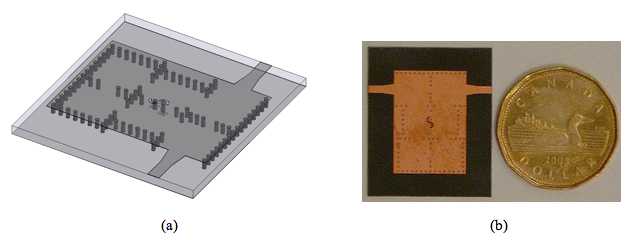
Figure 3 (right): SIW cross-coupled filter (a) with source-load coupling by using a negative coupling structure, and prototype photography (b)
In addition, the SIW and other SICs geometry can be used to design a wide range of antennas and phased arrays as well as multi-beam and multi-band antennas such as slotted waveguide antennas, high-order mode leaky-wave radiators, and planar beam-forming networks as well as planar lens [23, 24, 33, 34, 35].
3.3 System-on-substrate (SoS) approach
Since passive and active components can easily be made with the proposed SICs technique, it is possible to integrate all the components required for the transceiver front-end into the same substrate made by the same process. This is the system-on-substrate (SoS) approach, which allows us to design the radio and radar transceiver with a very high density integration. In this case, all of the passive components including antennas can be made on the substrate together with active elements [36]. Figure 4 shows the picture of a complete 24 GHz radar including two antennas prior to surface-mounting active parts, which was realized on the basis of the proposed SoS approach. This technique has been recently extended to the design of a complete 60 GHz active antenna–based receiver.
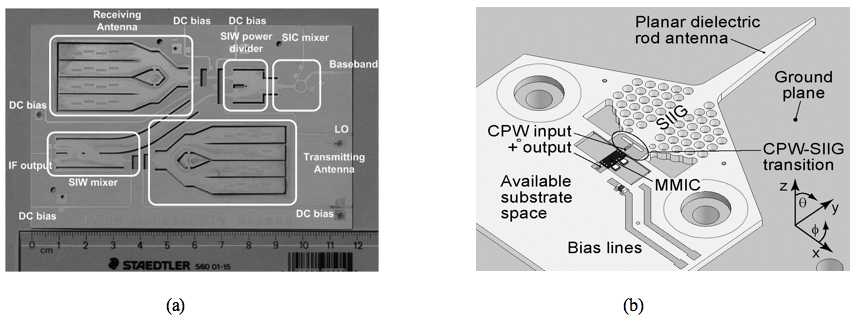
Figure 4 (left): Complete 24 GHz radar prototype without the showing of surface-mounted devices (a), and 60 GHz active radio front-end (b) on the basis of the system-on-substrate (SoS) approach
4. Conclusion and Future Outlook
This news report describes an emerging ICs technology called substrate integrated circuits (SICs) with a number of practical examples, which can be used in many interesting applications over a wide range of frequencies from RF to THz bands. This technology development has a very close relationship with the on-going research effort in searching for novel nano-structured and smart materials that will have a huge impact on the future of SICs. The SICs concept has been demonstrated for the development of systems-on-substrate (SoS), which provides a very large-scale high-density integration at very high frequencies.
It is widely known in the community of circuits and systems that the most important and visible feature in our current electronic circuits and systems is probably the wide use of lumped-element concepts such as capacity, inductor, and resistor. In fact, diodes and transistors also present a specific form of lumped-elements that operate in terms of voltages and currents. Those active devices may operate well into the THz range if nano-structured techniques are deployed but they are still lumped-elements in nature and thus pose fundamental limitations in their operation and performances. Therefore, there is a critical search for the next generation of “active devices” based on pure guided-wave and transmission line concepts, which will be in contrast to the well-established rule of lumped-elements such as the “size shrinking" with respect to wavelength in order to satisfy “voltage” and “current” circuit designs in the domain of electronics. This technology that remains to be discovered will definitely change the landscape of our future electronic and photonic circuits and systems, and this will be in direct relationship with the development of SICs. It can be anticipated that this SICs technology would bridge the gap between electronics and photonics.
5. Acknowledgement
The author is grateful to his former/current students, post-doctoral fellows, research associates, technicians and collaborators for their contributions that have made this novel technology development possible. He wishes to acknowledge the financial contributions of the NSERC of Canada, the FQRNT of Quebec and others in support of this work.
References
[1] K. C. Gupta, R. Garg, I. Bahl, and P. Bhartia, Microstrip Lines and Slotlines, 2nd edition, Artech House, Dedham, MA, 1996.
[2] S. N. Rainee, Coplanar Waveguide Circuits, Components and Systems, Wiley-Interscience, New York, 2001.
[3] R. A. Pucel, D. J. Massé, and C. P. Hartwig, “Losses in microstrip,” IEEE Trans. MTT, Vol. 16, No. 6, 1968, pp. 342-350.
[4] K. Wu, R. Vahldieck, J. Fikart, and H. Minkus, “The influence of finite conductor thickness and conductivity on fundamental and higher-order modes in Miniature Hybrid MIC's (MHMIC's) and MMIC's,” IEEE Trans. MTT, Vol. 41, No. 3 1993, pp. 421-430.
[5] K. Wu, “Hybrid three-dimensional planar/non-planar circuits for microwave and millimeter-wave applications: the state-of-the-art and challenges,” TELSIKS’97, Nis, Yugoslavia, Oct. 8-10, pp. 281-286 (invited paper).
[6] K. Wu and L. Han, “Hybrid integration technology of planar circuits and NRD-guide for cost-effective microwave and millimeter-wave applications,” IEEE Trans. MTT, Vol. 45, June 1997, pp. 946-954.
[7] K. Wu, J. Dallaire, and F. Boone, “Channelized non-radiative dielectric guide for hybrid and monolithic integration technology,” 1998 Asia-Pacific Microwave Conf. Proc. (APMC'98), Japan, Dec. 8-11, pp. 265-268.
[8] K. Wu, “Integration and interconnect techniques of planar and non-planar structures for microwave and millimeter-wave circuits - current status and future trend,” 2001 Asia-Pacific Microwave Conf. Proc. (APMC'01), Taiwan, pp. 411-416 (invited paper).
[9] D. Deslandes and K. Wu, “Integrated microstrip and rectangular waveguide in planar form,” IEEE Microwave and Wireless Components Letters, Vol. 11, Feb 2001, pp. 68-70
[10] Y. Cassivi, L. Perregrini, P. Arcioni, M. Bressan, K. Wu and G. Conciauro, “Dispersion characteristics of substrate integrated rectangular waveguide,” IEEE Microwave and Wireless Components Letters, Vol. 12, Sept. 2002, pp. 333-335.
[11] F. Xu, and K. Wu, “Guided-wave and leakage characteristics of substrate integrated waveguides,” IEEE Trans. MTT, Vol. 53, Jan. 2005, pp. 66-73.
[12] D. Deslandes and K. Wu, “Substrate integrated waveguide leaky-wave antenna: concept and design considerations,” 2005 Asia-Pacific Microwave Conf. Proc. (APMC'05), Dec. 4-7, Suzhou, China, pp. 346-349.
[13] D. Stephens, D. Young, and I.D. Robertson, “Design and performance of millimeter-wave substrate integrated waveguide filters,” IEEE Trans. MTT, vol. 53, Dec. 2005, pp.3832-3838.
[14] W. D’Orazio and K. Wu, “Substrate integrated waveguide circulators suitable for millimeter-wave integration,” IEEE Trans. Microwave Theory Tech., Vol. 54, Oct. 2006, pp. 3675-3680.
[15] J. J. Simpson, A. Taflove, A. Mix, and H. Heck, “Substrate integrated waveguide optimized for ultrahigh-speed digital interconnects,” IEEE Trans. MTT, Vol, 54, May 2006, pp. 1983-1990.
[16] B. Sanz Izquierdo, N. Grigoropoulos, and P. R. Young, “Ultra-wideband multilayer substrate integrated folded waveguides,” IEEE MTT-S International Microwave Symposium, San Francisco, June 2006.
[17] Y.-J. Cheng, W. Hong, and K. Wu, “Half mode substrate integrated waveguide (HM-SIW) directional filter,” IEEE Microwave and Wireless Components Lett., Vol. 17, July 2007, pp. 504-506.
[18] D. Deslandes, K. Wu, “Accurate modeling, wave mechanisms, and design considerations of substrate integrated waveguide,” IEEE Trans. Microwave Theory Tech., Vol. 54, June 2006, pp. 2516-2526.
[19] T. Djerafi, K. Wu, “Super-compact substrate integrated waveguide cruciform directional coupler,” IEEE Microwave and Wireless Components Lett., Vol. 17, Nov. 2007, pp. 757-759.
[20] S. Cheng, H. Yousef, and H. Kratz, “79 GHz slot antennas based on substrate integrated waveguide (SIW) in a flexible printed circuit board,” IEEE Trans. Antennas and Propagation, Vol. 57, no. 1, Jan. 2009, pp. 64-71.
[21] X.-P. Chen, K. Wu, and D. Drolet, “Substrate integrated waveguide filter with improved stopband performance for satellite ground terminal,” IEEE Trans. Microwave Theory Tech., Vol. 57, March 2009, pp. 674-683.
[22] Y.-J Cheng, K. Wu, and W. Hong, “Power handling capability of substrate integrated waveguide interconnects and related transmission line systems,” IEEE Trans. Advanced Packaging, Vol. 31, no. 4, Nov. 2008, pp. 900-909.
[23] A. Patrovsky and K. Wu, “Substrate Integrated Image Guide (SIIG)—a novel planar dielectric waveguide technology for millimeter-wave applications,” IEEE Trans. MTT, Vol. 54, June 2006, pp. 2872-2879.
[24] A. Patrovsky and K. Wu, “Substrate Integrated Image Guide (SIIG) array antenna for the upper millimeter-wave spectrum,” IEEE Trans. Antennas and Propagation, Vol. 55, no. 11, November 2007, pp. 2994-3001.
[25] Y.-J. Cheng, W. Hong, and K. Wu, “Half mode substrate integrated waveguide (HMSIW) directional filter,” IEEE Microwave and Wireless Components Lett., Vol. 17, July 2007, pp. 504-506.
[26] B. Liu, W. Hong, Y. Zhang, H. J. Tang, X.-X, Yin, and K. Wu, “Half-mode substrate integrated waveguide 180 3-dB directional couplers,” IEEE Trans. Microwave Theory Tech., Vol. 55, no. 12, December 2007, pp. 2586-2592.
[27] A. Yoji, U. Hiromitsu, Y. Naofumi, M. Moriyasu, and K. Yoshihiko, “Single mode nonradiative dielectric waveguide using split dielectric strips,” IEIC Technical Report (IEICE), Vol. 106, No. 48, 2006, pp. 59-63.
[28] D. Deslandes and K. Wu, “Analysis and design of current probe transition from grounded coplanar to substrate integrated rectangular waveguides,” IEEE Trans. MTT, Vol. 53, Aug. 2005, pp.2487-2494.
[29] A. Patrovsky, M. Daigle, and K. Wu, “Coupling mechanism in hybrid SIW-CPW forward couplers for millimeter wave substrate integrated circuits,” IEEE Trans. Microwave Theory Tech., Vol. 56, no. 11, November 2008, pp. 2594-2601.
[30] Y. Ding and K. Wu, “Substrate integrated waveguide-to-microstrip transition in multilayer substrate,” IEEE Trans. Microwave Theory Tech., Vol. 55, no. 12, December 2007, pp. 2839-2844.
[31] X.-P. Chen, K. Wu, “Low-loss ultra-wideband transition between conductor-backed coplanar waveguide and substrate integrated waveguide,” 2009 IEEE MTT-S Inter. Microwave Symp., to be published.
[32] X.-P. Chen and K. Wu, “Substrate integrated waveguide cross-coupled filter with negative coupling structure,” IEEE Trans. Microwave Theory Tech., Vol. 56, Jan. 2008, pp. 142-149.
[33] Y.-J. Cheng, W. Hong, K. Wu, Z.-Q. Kuai, C. Yu, J.-X. Chen, J.-Y. Zhou, and H.-J. Tang, “Substrate integrated waveguide (SIW) Rotman Lens and its Ka-band multibeam array antenna applications,” IEEE Trans. Antennas and Propagation, Vol. 56, Aug. 2008, pp. 2504-2513.
[34] Y.-J. Cheng, W. Hong, and K. Wu, “Design of a monopulse antenna using a dual V-type linearly tapered slot antenna (DVLTSA),” IEEE Trans. Antennas and Propagation, Vol. 56, no. 9, Sept. 2008, pp. 2903-2908.
[35] F. Xu, K. Wu, and X. P. Zhang, “Periodic leaky-wave antenna for millimeter waves based on substrate integrated waveguide,” IEEE Trans. Antennas and Propagation, to be published.
[36] Z.-L. L and K. Wu, “24 GHz frequency-modulation continuous-wave radar front-end system-on-substrate,” IEEE Trans. Microwave Theory Tech., Vol. 56, no. 2, Feb. 2008, pp. 278-285.
Ke Wu, Poly-Grames Research Center, Department of Electrical Engineering, Center for Radio-frequency Electronics Research (CREER) of Québec, Ecole Polytechnique, Canada (Email: ke.wu@polymtl.ca)