
TECHNOLOGY NEWS
A Throughput-Centric Paradigm for On-FPGA Communication Systems
1. Introduction
Interconnect performance is rapidly deteriorating with the continuous scaling in technology processes. As predicted by the International Technology Roadmap for Semiconductors (ITRS) in Fig. 1, there is a significant performance gap between interconnection RC delay and the gate delay, and this gap will be increasing exponentially (9:1 with the 65 nm technology according to ITRS 2005 report [1]).
The interconnect challenge is exacerbated in the Field-Programmable Gate Array (FPGA), which is a type of ASIC where the hardware can be programmed post-fabrication. FPGAs offer great versatility and flexibility compared to standard ASICs and its popularity as rapid-prototyping [2], high-performance computing [3] and embedded system design [4] platform grows rapidly. With a unique reconfigurable architecture, interconnections in FPGA are generally constructed from segments of interconnect fabrics and programmable switches. Programmability introduces great flexibility in post-fabrication and speed up the system development cycle, but at a cost of slower performance and higher dissipating of energy when compared to its ASIC counterpart. This is especially the case for global interconnections, which span a large physical distance across the chip. Long interconnection with multiple concatenated wire segments would result in inferior performance [5]. Although more components and modules can be fitted into a single FPGA, intra-FPGA communication system with these long interconnections would become a bottleneck to the overall system performance [6].
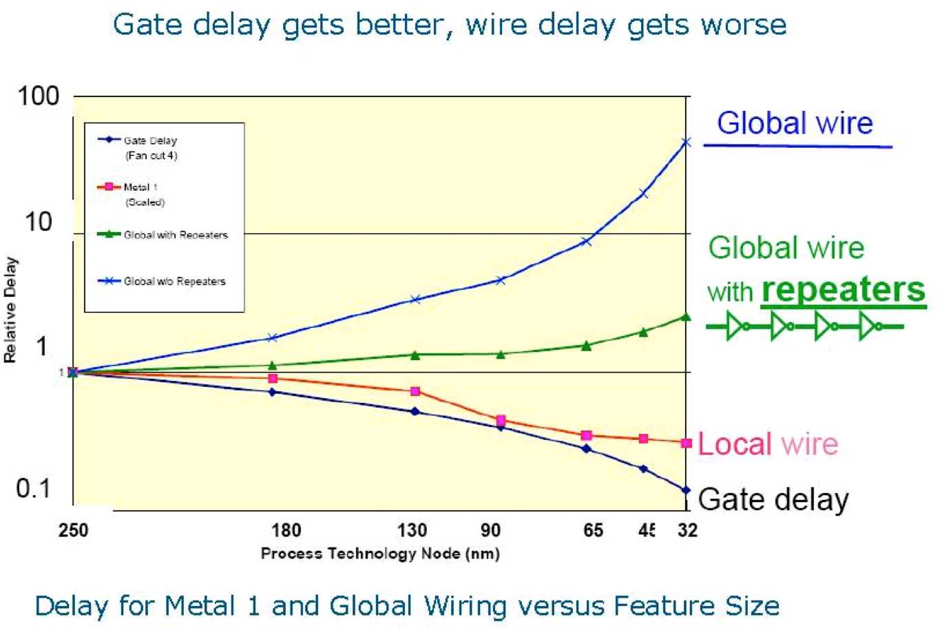
Fig. 1: Projected relative delay for local and global wires
and for logic gates in technologies of the near future [1]
In-depth understanding of the reconfigurable architecture is of vital importance and provides an opportunity to study the exploitation of the underlying FPGA architecture for intra-chip communication purposes. This article discusses new interconnect models [10-11] and novel design methods [12] that aim to maximize the throughput performance in on-chip communication systems, and in particular how these methods may be adapted to incorporate and exploit reconfigurable architectures. A comprehensive survey on design methods for on-FPGA communication can be found in [6].
-
2. Fringed Interconnects and Bandwidth Degradation
In many commercial and state-of-the-art FPGAs [13-14], different types of interconnects are available in the routing channel for realizing different interconnections and nets. Having these heterogeneous interconnects is very versatile and is effective for accommodating different requirements of the design. Interestingly, although there are different type of interconnects available, long wires are the most frequently used to realize the interconnections between two separated modules while other types of interconnects are used for interconnections within the modular block. This can be easily explained by the fact that using long wires is efficient for long distance routing.
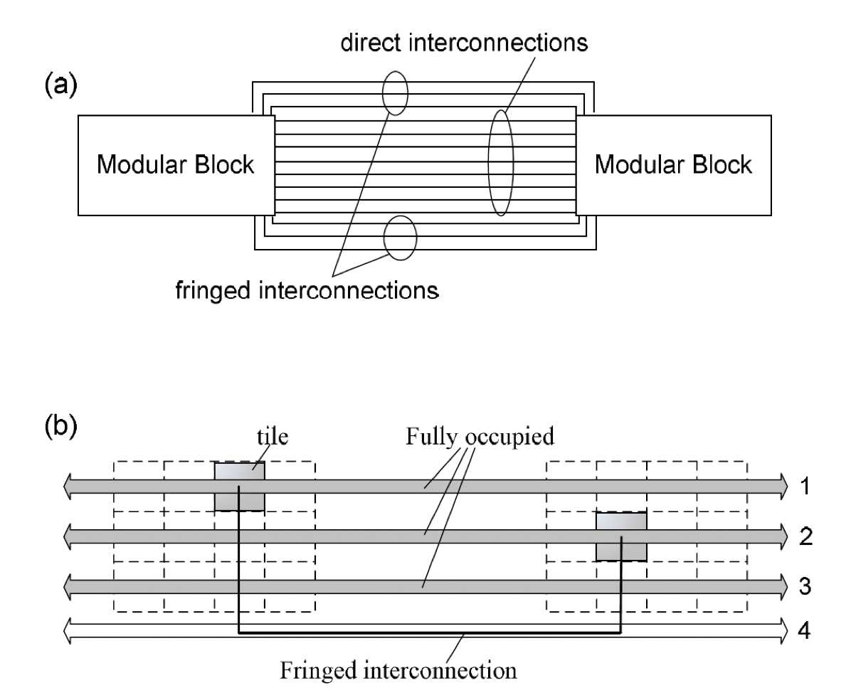
Fig. 2: (a) An abstract view of both direct and fringed interconnections in a link after the placement and routing steps. (b) An typical example of a fringed interconnection
The fringed interconnects and limited routing resources would result a bandwidth degradation in communication link. In other words, an increase in bit-width will increase the delay and, thus, adversely affect the increase in bandwidth. An example is shown in Fig. 3, which sketches a general observation of the bandwidths of parallel lines for different bit-widths. Dashed line represents the ideal bandwidth and the solid line represents the degraded bandwidth after the place-and-route in a reconfigurable architecture.
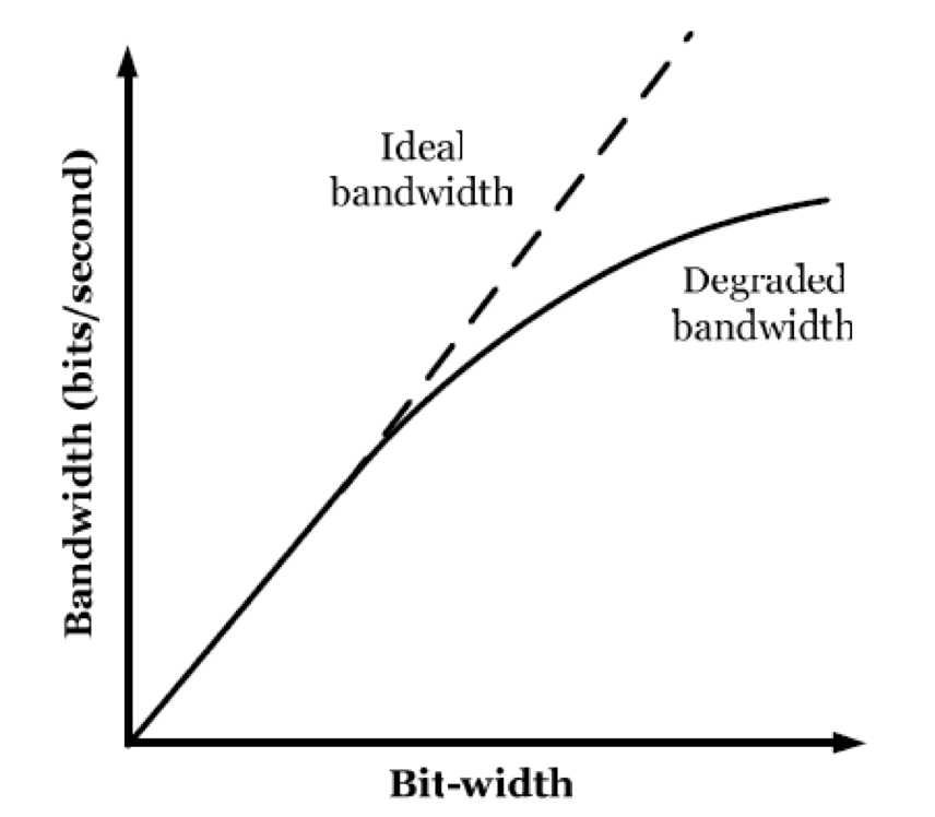
Fig. 3: The ideal and degraded bandwidths against bit-width of a communication link in FPGAs
3. On-FPGA Wave-Pipelined Signalling
Despite of the irregularity and idiosyncratic nature of FPGA long interconnections, buffers were embedded at switches to speed up the signal propagation. With the help of these buffers, the long interconnections can be modeled as multiple stages of RC transmission line, which facilitate the realization of wave-pipelined signaling [5]. In wave-pipelined signaling, multiple bits are allowed to traverse simultaneously along the line, thus a significant throughput improvement can be obtained. For many complex applications, bandwidth is the main concern for communication between modules or processors. A conventional interconnect has its bandwidth dictated by the RC time constant (or characteristic impedance) of the wire, thus limiting the data throughput. Using wave-pipelined signaling, the data throughput can exceed the limit imposed by the RC time constant [12].
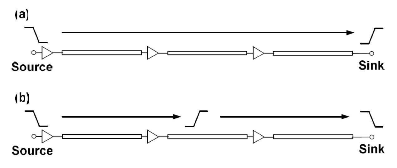
Fig. 4: Signal transmission using (a) delay-based and
(b) wave-pipelined schemes
Conventional delay-based signalling uses a synchronous mechanism that a new bit of data will be transmitted from the source only if the last bit of data has arrived the sink. Therefore, the throughput of interconnect for this approach will be the reciprocal of the interconnect delay. Fig. 4(a) shows the mechanism of delay-based signalling. A new data bit, as illustrated by the falling edge in the figure, is started to be transmitted when the previous data bit has arrived at the sink. The throughput of an interconnect can be increased by increasing the data injection rate. The source injects a new data bit into the link even when the previous data bit has not arrived at the sink (as shown in Fig. 4(b)). In this way, the throughput of the link can be greatly improved, as multiple bits are traversing along the line simultaneously.
4. Conclusion
Design for bandwidth re-emphasizes on utilizing silicon resources for signal and information transportation instead of for arithmetic and computational purposes as in FPGA systems. Bandwidth can be enhanced by designing new signalling schemes via exploiting semiconductor physical characteristics. There are other new methodologies and techniques that dedicate for on-FPGA communication architectures including on-FPGA time-multiplexing network [15], high-throughput surfing interconnects [16] and FPGA-NoC architectures [17]. These new throughput-centric approaches together provide a promising high bandwidth solution that can potentially mitigate the future on-chip communication challenges.
Acknowledgement
The author is grateful to the support of the Croucher Foundation Scholarship.
References
[1] D. Edenfeld, A. B. Kahng, M. Rodgers, and Y. Zorian, “Technology roadmap for semiconductors”, Computer, vol. 37(1), pp. 47–56, 2004.
[2] T.J. Todman, G.A. Constantinides, S.J.E. Wilton, O. Mencer, W. Luk and P.Y.K. Cheung, “Reconfigurable computing: architectures and design methods”, IET Proc. - Computers and Digital Techniques, vol. 152(2), pp. 193-207, 2005
[3] M. Herbordt, T. VanCourt, Y. Gu, B. Sukhwani, A. Conti, J. Model, and D. DiSabello, “Achieving High Performance with FPGA-Based Computing”, Computer, vol. 40(3), pp. 50-57, 2007.
[4] L. Shang, R. P. Dick, and N. K. Jha, "SLOPES: Hardware-software co-synthesis of low power real-time distributed embedded systems with dynamically reconfigurable FPGAs", in Proc. Asia and South Pacific Design Automation Conference, 2007.
[5] T. Mak, C. D’Alessandro, P. Sedcole, P. Cheung, A. Yakovlev, and W. Luk, “Global interconnections in FPGAs: Modeling and performance analysis”, in Proc. Of International Workshop on System Level Interconnect Prediction (SLIP), 2008.
[6] T. Mak, P. Sedcole, P. Cheung, and W. Luk, “On-FPGA communication architectures and design factors”, in Proc. IEEE International Conference on Field Programmable Logic and Applications (FPL), 2006.
[7] L. Benini and D. Bertozzi. Network-on-chip architectures and design methods. IEE Proc.-Comput. Digit. Tech., 152(2):261–272, 2005.
[8] W.J. Dally and B. Towles, “Route packets, not wires: On-chip interconnection networks”, in Proc. of Design Automation Conference (DAC), 2001.
[9] Giovanni De Micheli and Luca Benini. Networks on Chips: Technology and Tools. Morgan Kaufmann, 2006.
[10] T. Mak, P. Sedcole, P.Y.K. Cheung, and W. Luk, “Average interconnection delay estimation for on-FPGA communication links”, Electronic Letters, 43(17):918–920, 2007.
[11] T. Mak, P. Sedcole, P. Cheung, and W. Luk, “Interconnection lengths and delays estimation for communication links in FPGAs”, in ACM International Workshop on System Level Interconnect Prediction, 2008.
[12] Terrence Mak, Pete Sedcole, Peter Y.K. Cheung, and Wayne Luk, “Wave-pipelined signalling for On-FPGA communication”, in Proc. IEEE International Conference on Field Programmable Technology (FPT), 2008.
[13] Xilinx. Virtex-4 Data Sheets. 2005.
[14] Altera. Stratix II Device Family Data Sheet. 2005.
[15] R. Francis, S. Moore and R. Mullins, “A Network of Time-Division Multiplexed Wiring for FPGAs”, in Proc. of the ACM/IEEE International Symposium on Networks-on-Chip, 2008
[16] P. Teehan, G. Lemieux, and M. Greenstreet, “Towards Reliable 5Gbps Wave-pipelined and 3Gbps Surfing Interconnect in 65nm FPGAs'”, in Proc. ACM/SIGDA International Symposium on Field-Programmable Gate Arrays, 2009.
[17] K. Goossens, M. Bennebroek, J. Y. Hur, and M.-A.Wahlah, “Hardwired networks on chip in FPGAs to unify functional and configuration interconnects”, in Proc, IEEE International Symposium on Networks-on-Chip, 2008.
Terrence Mak, Department of Electrical and Electronic Engineering, Imperial College London, UK (Email: t.mak@imperial.ac.uk)

Recommended by H. Iu.