Our Editors-in-Chief’s Top Picks
The Editors-in-Chief of our CASS publications have selected some noteworthy papers from the recent issues of our journals:
IEEE Transactions on Circuits and Systems II: Express Briefs
Paper 1:
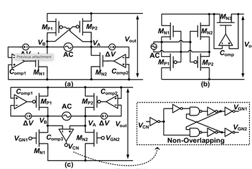
X. Liu, B. Moradi and H. Aghasi, "A Single-Switch 3.1–4.7 GHz 194.52-dB FoM Class-D VCO With 495μW Power Consumption," IEEE Transactions on Circuits and Systems II: Express Briefs, vol. 71, no. 10, pp. 4451-4455, Oct. 2024, doi: 10.1109/TCSII.2024.3407842. https://ieeexplore.ieee.org/document/10543114
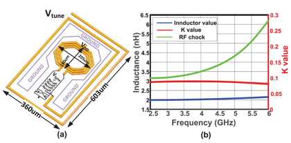
Summary: This work presents an ultra-low-power class-D voltage-controlled oscillator (VCO) designed for GHz applications that mandate decent phase noise performance. A waveform-centric approach of phase noise reduction by controlling the ratio between the floating and single-ended (SE) capacitors in an oscillator tank is proposed.
Paper 2:
M. Abe, H. Kokubun, T. Aida, K. Goto and K. Kobayashi, "A high-speed digital filter LSI for video signal processing," IEEE Journal of Solid-State Circuits, vol. 22, no. 3, pp. 396-402, June 1987, doi: 10.1109/JSSC.1987.1052738. https://ieeexplore.ieee.org/document/1052738

Summary: This brief presents a 400 V monolithically integrated half-bridge buck converter in a 650 V GaN-on-SOI technology. It integrates gate drivers, switching logic and power management into a single HV ASIC. A 36 ns comparator and a configurable timer enable use as a ripple-based Constant-On-Time (COT) regulator with 1.4% transient load regulation for a 75% load step. A peak efficiency of 92.0% converting from 400 V to 48 V, 95.5% peak efficiency and 15.7 W mm−2 power density are achieved.
Paper 3:
J. -Y. Park and J.-W. Nam, "A 4.3 GS/s Time-Interleaved ΔΣ DAC With Temperature-Insensitive Bias and Harmonic Cancellation for Qubit Control," IEEE Transactions on Circuits and Systems II: Express Briefs, vol. 71, no. 11, pp. 4663-4667, Nov. 2024, doi: 10.1109/TCSII.2024.3470111. https://ieeexplore.ieee.org/document/10699418
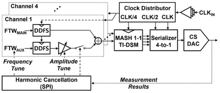
Summary: A qubit-control waveform generator with a 4-channel time-interleaved ΔΣ DAC is presented. A digital-to-analog converter (DAC) at 4.3 GS/s with an oversampling rate of 8 is fabricated in 65 nm CMOS technology. To enhance the linearity of the DAC, harmonic cancellation is proposed. Time-interleaving is applied in a ΔΣ modulator to widen the bandwidth. A high operational speed is also achieved through an unrolling technique to the direct digital frequency synthesis (DDFS) digital core. The signal-to-noise distortion ratio (SNDR) and the spurious free dynamic range (SFDR) after enabling harmonic cancellation are respectively 30.62 dB and 47.03 dB at 100 K temperature.
IEEE Transactions on Circuits and Systems for Video Technologies
Paper 1:
S. Long, Q. Zhou, C. Ying, L. Ma and Y. Luo, "Rethinking Domain Generalization: Discriminability and Generalizability," IEEE Transactions on Circuits and Systems for Video Technology, vol. 34, no. 11, pp. 11783-11797, Nov. 2024, doi: 10.1109/TCSVT.2024.3422887.
https://ieeexplore.ieee.org/document/10583916
Summary: This paper presents a novel framework, namely, Discriminative Microscopic Distribution Alignment (DMDA) for domain generalization (DG) by using a new perspective that concurrently imbues features with discriminability and robust generalizability. DMDA incorporates two main components: Selective Channel Pruning (SCP) and Micro-level Distribution Alignment (MDA). Concretely, SCP attempts to curtail redundancy within neural networks, prioritizing stable attributes conducive to accurate classification. This approach alleviates the adverse effect of spurious domain-invariance and amplifies the feature discriminability. Besides, MDA accentuates micro-level alignment within each class, going beyond mere category-level alignment. This strategy accommodates sufficient generalizable features and facilitates within-class variations. Experiments on four benchmark datasets corroborate that DMDA achieves comparable results to state-of-the-art methods in DG.
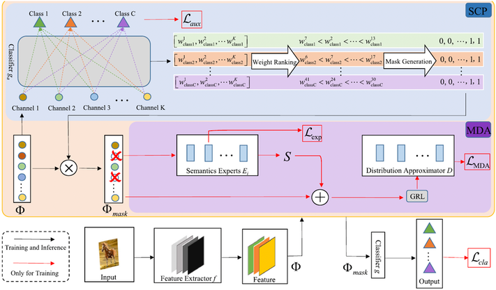
The Discriminative Microscopic Distribution Alignment (DMDA) framework. The features generated by the feature extractor are initially transmitted to the Selective Channel Pruning (SCP) module to create channel-wise masks for the purpose of eliminating unstable channels. Following this, the features undergo pruning based on the channel-wise masks. Subsequently, Micro-level Distribution Alignment (MDA) is employed to execute micro-level distribution alignment rooted in the latent semantics of the pruned features, which are generated by additional semantics experts.
Paper 2:
X. Sun, G. Cheng, H. Li, H. Peng and J. Han, "Task-Specific Importance-Awareness Matters: On Targeted Attacks Against Object Detection," IEEE Transactions on Circuits and Systems for Video Technology, vol. 34, no. 11, pp. 11619-11629, Nov. 2024, doi: 10.1109/TCSVT.2024.3425655.
https://ieeexplore.ieee.org/document/10589915
Summary: This paper concentrates on Targeted Attacks on Object Detection (TAOD) in optical remote sensing images, and pays attention to a fundamental question, how to deploy TAOD via the raw predictions (the predictions before non-maximum suppression) of a victim detector. In this regard, this paper departs from widely adopted task-independent importance measurements and hard-weighted ensemble optimization schemes present in existing methods. Instead, this work first defines the task-specific importance score, which considers both the qualities and the attack costs of predictions. Further, the Task-Specific Importance-Aware Candidate Predictions Selection Scheme (TSIA-CPSS) is proposed alongside the Soft-Weighted Ensemble Optimization Scheme (SW-EOS). A total of eleven detectors on DIOR and DOTA, two commonly employed benchmarks, are included to comprehensively evaluate the approach proposed in this paper. The effectiveness of the proposed approach is substantial for vanilla TAOD, and can also be better generalized to extended scenarios, which encompasses random TAOD, TAOD on oriented object detection, and targeted patch attacks.
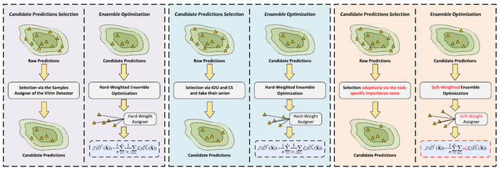
Comparisons regarding two key steps (CPSS and EOS) between two works in the literature (middle), and the TSIAA proposed solution (right). TSIAA essentially diverges from existing approaches in two aspects: (i) TSIAA selects candidate predictions based on the defined task-specific importance score; (ii) TSIAA assigns individual weights calculated by the importance scores, employing a soft-weighted ensemble optimization scheme.
Paper 3:
Q. Chen et al., "SDPL: Shifting-Dense Partition Learning for UAV-View Geo-Localization," IEEE Transactions on Circuits and Systems for Video Technology, vol. 34, no. 11, pp. 11810-11824, Nov. 2024, doi: 10.1109/TCSVT.2024.3424196.
https://ieeexplore.ieee.org/document/10587023
Summary: This paper introduces a simple yet effective part-based representation learning, called shifting-dense partition learning (SDPL). In particular, a dense partition strategy (DPS) is proposed, dividing the image into multiple parts to explore contextual information, while explicitly maintaining the global structure. To handle scenarios with non-centered targets, a shifting-fusion strategy is proposed that generates multiple sets of parts in parallel based on various segmentation centers, and then adaptively fuses all features to integrate their anti-offset ability. Experiments show that SDPL is robust to position shifting, and performs competitively on two prevailing benchmarks, University-1652 and SUES-200. In addition, SDPL shows satisfactory compatibility with a variety of backbone networks like ResNet and Swin.
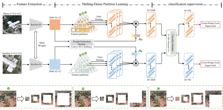
Overview of the SDPL framework. A-C (bottom): Diagrams of dense partition strategy with various segmentation centers. During testing, part-level image representation is extracted before classification layer in classifier module, and measures similarity by Euclidean distance
IEEE Journal on Emerging and Selected Topics in Circuits and Systems
Paper 1:
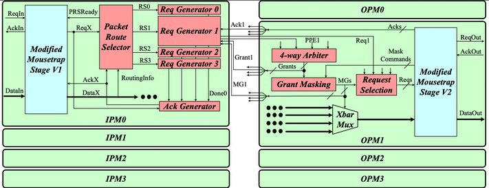
Z. Su et al., "An Ultra-Low Cost and Multicast-Enabled Asynchronous NoC for Neuromorphic Edge Computing," IEEE Journal on Emerging and Selected Topics in Circuits and Systems, vol. 14, no. 3, pp. 409-424, Sept. 2024, doi: 10.1109/JETCAS.2024.3433427. https://ieeexplore.ieee.org/abstract/document/10609786
Summary: Motivated by the need for more efficient computing, biological brains are inspiring the development of spiking neural-network-based neuromorphic processors for energy-constrained edge devices. This work addresses a critical bottleneck in neuromorphic systems: the communication architecture, proposing a specialized network-on-chip (NoC) design optimized for event-driven, short-message routing. The result is a NoC that achieves energy savings of 42% to 71% compared to a state-of-the-art NoC in real multi-core neuromorphic processors.
Paper 2:
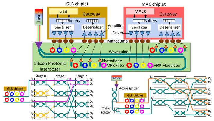
E. Taheri, M. Amin Mahdian, S. Pasricha and M. Nikdast, "SwInt: A Non-Blocking Switch-Based Silicon Photonic Interposer Network for 2.5D Machine Learning Accelerators," IEEE Journal on Emerging and Selected Topics in Circuits and Systems, vol. 14, no. 3, pp. 520-533, Sept. 2024, doi: 10.1109/JETCAS.2024.3429354. https://ieeexplore.ieee.org/document/10599539
Summary: Machine Learning (ML) accelerators need to be more efficient and scalable to meet growing computational demands without high fabrication costs. Towards this goal, this paper proposes SwInt, a 2.5D chiplet-based silicon photonic interposer with a switch-based network for energy-efficient, scalable data movement. The evaluations show that SwInt achieves a 59.7% energy efficiency improvement over existing silicon photonic interposers.
Paper 3:
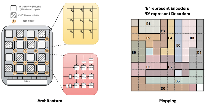
A. Jaiswal et al., "HALO: Communication-Aware Heterogeneous 2.5-D System for Energy-Efficient LLM Execution at Edge," IEEE Journal on Emerging and Selected Topics in Circuits and Systems, vol. 14, no. 3, pp. 425-439, Sept. 2024, doi: 10.1109/JETCAS.2024.3427421
Summary: Large Language Models (LLMs) are fantastic but eat up too much energy even during inference. We propose communication-aware heterogeneous 2.5D systems with both ReRAM and CMOS devices to perform different types of multiplications for LLM in an energy-efficient manner.
The proposed system shows 972× improvement in latency and 1600× improvement in energy consumption with respect to NVIDIA Jetson Orin Nano.
IEEE Open Journal of Circuits and Systems
Paper 1:
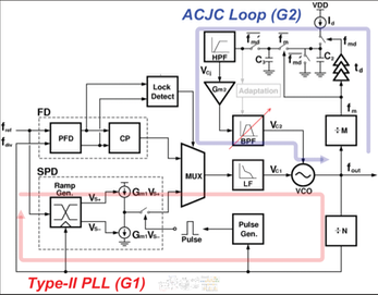
Y. -P. Huang, Y. -S. Lu and W. -Z. Chen, "A 10 GHz Dual-Loop PLL With Active Cycle-Jitter Correction Achieving 12dB Spur and 29% Jitter Reduction," IEEE Open Journal of Circuits and Systems, vol. 5, pp. 291-301, 2024, doi: 10.1109/OJCAS.2024.3416397. https://ieeexplore.ieee.org/document/10561565
Summary: This paper presents the design of a 10 GHz dual-loop PLL with active cycle-jitter correction. In the main loop of the PLL, a sampling PD is utilized to suppress the in-band noise to reach the reference noise floor.
Paper 2:
S. Song et al., "Low-Power On-Chip Energy Harvesting: From Interface Circuits Perspective," IEEE Open Journal of Circuits and Systems, vol. 5, pp. 267-290, 2024, doi: 10.1109/OJCAS.2024.3423484. https://ieeexplore.ieee.org/document/10585308
Summary: This paper reviews existing energy harvesting modalities, including photovoltaic, piezoelectric, pyroelectric, electromagnetic, and vibration, together with circuit techniques of interfacing power management circuits for energy harvesters.
Paper 3:
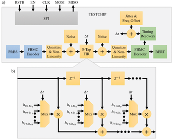
J. Cosson-Martin, J. Salinas, H. Shakiba and A. Sheikholeslami, "FBMC vs. PAM and DMT for High-Speed Wireline Communication," IEEE Open Journal of Circuits and Systems, vol. 5, pp. 243-253, 2024, doi: 10.1109/OJCAS.2024.3410020. https://ieeexplore.ieee.org/document/10549936
Summary: This paper demonstrates the first silicon-verified FBMC encoder and decoder designed to emulate beyond 224Gb/s wireline communication.
________________
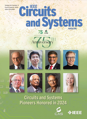
IEEE CAS Magazine Fourth Quarter Issue 2024
Feature
C. Power, R. B. Staszewski and E. Blokhina, "Charge-Based Single-Shot Readout Systems in Quantum Computing [Feature]," IEEE Circuits and Systems Magazine, vol. 24, no. 4, pp. 42-64, Fourthquarter 2024, doi: 10.1109/MCAS.2024.3401618.
CAS Education
C. K. Singh and G. C. Temes, "R-C Ladder Design: A Tutorial [CAS Education]," IEEE Circuits and Systems Magazine, vol. 24, no. 4, pp. 65-69, Fourthquarter 2024, doi: 10.1109/MCAS.2024.3462661.
D. Biolek, "Leon Chua and His Double-Eight Fingerprint [CAS Education]," in IEEE Circuits and Systems Magazine, vol. 24, no. 4, pp. 70-78, Fourthquarter 2024, doi: 10.1109/MCAS.2024.3462298.
and more …
________________
The TCASAI Inaugural Issue is Now Available!
We are thrilled to announce the inaugural issue of IEEE Transactions on Circuits and Systems for Artificial Intelligence (TCASAI) is now available.
TCASAI is co-sponsored by IEEE Circuits and Systems Society (IEEE CASS), IEEE Council on Electronic Design Automation (IEEE CEDA), IEEE Solid-State Circuits Society (IEEE SSCS) and technically co-sponsored by the IEEE Electron Devices Society (EDS) and the IEEE Nanotechnology Council.
As the first IEEE periodical dedicated to artificial intelligence (AI) hardware, the IEEE Transactions on Circuits and Systems for Artificial Intelligence (TCASAI) publishes contributions related to circuits and systems for artificial intelligence, including circuit and electronic system design, implementation, and demonstration.
The IEEE TCASAI is also thrilled to announce its inaugural editorial board, which can be viewed here.
________________
IEEE JETCAS Call for Papers: 2.5D/3D Chiplet Circuits and Systems, EDA, Advanced Packaging, and Test
Scope and Purpose
The task of integrating an increasing number of transistors onto a single chip is becoming increasingly arduous and costly. To counter this challenge, chiplet technology has captured the interest of both industry and academia. A chiplet is a small integrated circuit (IC) with a well-defined function, designed to be incorporated alongside other chiplets within a single package as a multi-die stack. Despite the current interest in a chiplet-based design approach, the associated technology faces numerous challenges that are influencing its development trajectory. This special issue is dedicated to showcasing the latest technological advancements in the field of chiplet technology and its applications.
In general, the chiplet interconnects faces design challenges such as achieving high bandwidth, low latency, high energy efficiency, high edge bandwidth density, low bit error rate, etc. There are existing standards for chiplet with no consideration on compatibility with each other at PHY layer specification, this raises the implementation cost of IP vendors and SoC designers.
Designing a chip based on the chiplet approach presents the challenge of how to effectively split a monolithic design into individual chiplets. An improper division will negatively impact the chip's performance and power efficiency. Furthermore, SoC designers must carefully consider the design of the system bus or I/O connected by chiplet interconnects, and keep the underlying structure remains transparent to the upper-layer software.
When developing a chip based on the chiplet approach, the SoC designer will meet the lack of comprehensive EDA tool coverage from front-end to back-end. For example, there are no EDA tools for multi-chiplets co-simulation in the front-end phase. They must leverage existing EDA tools that were initially designed for the development of monolithic SoC designs. Although multi-physics field co-simulation is utilized to identify potential risks before the tape-out phase, it is more beneficial and cost-effective to detect and mitigate issues during the front-end phase.
While chiplets are typically considered to be connected by interposers in advanced packaging, new methods such as silicon bridges have garnered public attention due to their lower cost. Hybrid bonding is also emerging as a promising technique for its extremely high density. 3D stacked ICs based on the chiplet approach draw more attention for their efficient way to integrate functional chiplets, but also result in more problems such as thermal.
2.5D- and 3D-stacked ICs based on the chiplet approach have many more potential test moments than conventional chips. Every test that is executed adds cost, and therefore, executing all these tests might lead to overkill and excessive test costs. However, not executing tests could lead to even higher costs. At the same time, pre-bond testing of the non-bottom dies is a challenging task, and we need to rely on a cooperative design-for-test infrastructure in the die-under-test and all dies below it.
The objective of this special issue is to give a systematic view of chiplet technology from many aspects, to find possible solutions for challenges, and to compile the latest research findings from researchers in the field.
Topics of Interest
To give a comprehensive introduction to this field, we are soliciting paper submissions presenting the latest developments in SoC architecture for chiplet-based IC and chiplets, chiplet interconnects, dedicated EDA tools along the entire design trajectory, 2.5D/3D advanced packaging, 2.5D/3D test and DfT. This special issue’s area of interest includes (but is not limited to) the following topics:
- Architecture exploration for chiplet-cased ICs
- System and technology co-optimization (STCO) for chiplet and advanced packaging
- System bus design in chiplet-based ICs
- General purpose computing chiplet
- Accelerator chiplet
- High-speed and low power I/O chiplet
- Multi-protocol combination design in I/O chiplet
- High-bandwidth memory chiplets
- High-speed design for chiplet interconnects
- Energy-efficient design for chiplet interconnects
- Multi-standard support in chiplet interconnects
- Adaptable I/O design for chiplet interconnects
- Floorplanning, partitioning, placement and routing optimization for chiplet-based IC by AI/ML
- Interconnect planning and synthesis
- Package/3D-IC placement and routing
- Extraction, TSV, and package modeling
- Deterministic/statistical timing analysis and optimization for chiplet-based IC
- Multi-chiplet functional co-simulation
- Multi-physics field co-simulation
- 2.5D/3D packaging and platforms
- Si/Glass/Organic-based interposer
- Si/Glass/Organic-based RDL
- Fanout wafer level and panel level packaging
- Hybrid bonding
- New chiplet and advanced packaging concepts and platforms
- Chiplet and stack description languages for advanced packaging
- SI and PI design for chiplet and advanced packaging
- Thermal design and materials in chiplet and advanced packaging
- Electromagnetic compatibility design in chiplet and advanced packaging
- Yield and cost estimation of stacked dies for chiplet and advanced packaging
- Stress, warpage, and reliability issue for chiplet and advanced packaging
- Built-In self-test (and repair) for chiplet interconnects
- Defects in chiplet Interconnects
- Design-for-test for and repair of chiplet interconnects
- DfT architectures for chiplet-based ICs
- EDA design-to-test flow for chiplet interconnects
- Failure analysis for chiplet interconnects
- Fault-tolerant design for chiplet interconnects
- Interposer testing
- Pre-, mid- and post-bond testing
- Reliability of chiplet interconnects
- Standards for chiplet interconnect test and repair, incl. IEEE Std P3405
- Standards for chiplet testing, incl. IEEE Std 1838
- Test flow optimization for chiplet interconnects
- Test pattern generation for chiplet interconnects
- Yield of stacked dies and their Interconnects
Submission procedure:
Prospective authors are invited to submit their papers following the instructions provided on the IEEE JETCAS website: https://ieee-cas.org/publication/JETCAS/manuscript-submission-guide. The submitted manuscripts should not have been previously published, nor should they be currently under consideration for publication elsewhere.
The IEEE JETCAS submission site is https://ieee.atyponrex.com/journal/jetcas.
Important dates
- 3 March 2025: Manuscript submissions due
- 21 April 2025: First round of reviews completed
- 2 June 2025: Revised manuscripts due
- 30 June 2025: Second round of reviews completed
- 21 July 2025: Final manuscripts due
Request for information
Corresponding Guest Editor: Qinfen Hao (haoqinfen@ict.ac.cn)
Guest Editors:
Qinfen Hao
Chinese Academy of Sciences
(haoqinfen@ict.ac.cn)
Kuan-Neng Chen
National Yang Ming Chiao Tung University
(knchen@nycu.edu.tw)
Sandeep Kumar Goel
TSMC
(skgoel@tsmc.com)
Hai Li
Duke University
(hai.li@duke.edu)
Erik Jan Marinissen
imec
(Erik.Jan.Marinissen@imec.be)
______________________________
Latest Tables of Contents of CAS Sponsored Journals
The latest issues of our CAS sponored journals have been published and the tables of contents can be accessed through the following links:

- IEEE Transactions on Circuits and Systems I: Regular Papers
- IEEE Transactions on Circuits and Systems II: Express Briefs
- IEEE Transactions on Circuits and Systems for Video Technology
- IEEE Journal on Emerging and Selected Topics in Circuits and Systems
- IEEE Circuits and Systems Magazine
- IEEE Transactions on Biomedical Circuits and Systems
- IEEE Design and Test Magaz
