Our Editors-in-Chief’s Top Picks
The Editors-in-Chief of our CASS publications have selected some noteworthy papers from the recent issues of our journals:
IEEE Transactions on Circuits and Systems I: Regular Papers
Paper 1:
C. Kumar and S. Pavan, "Weak Nonlinearities in Active Filters and Continuous-Time Pipeline ADCs," IEEE Transactions on Circuits and Systems I: Regular Papers, vol. 72, no. 12, pp. 7565-7577, Dec. 2025, doi: 10.1109/TCSI.2025.3571932
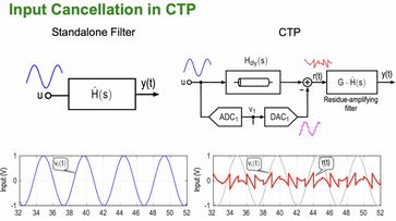
Summary: Traditional ADCs rely on a stand-alone analog anti-aliasing filter to suppress out-of-band signals prior to sampling. While essential, this filter can be power-hungry and is often a major source of distortion. Continuous-time pipeline (CTP) ADCs integrate the anti-aliasing function directly into the conversion process, effectively replacing the filter–ADC cascade with a single unified system. This architectural shift raises an important question regarding the impact of practical amplifier imperfections on linearity. In this paper, we analyze the effect of weak amplifier nonlinearities and demonstrate that an appropriately designed CTP can achieve inherently superior linearity compared to an equivalent traditional solution operating under identical noise and power constraints.
Paper 2:
S. Li et al., "An Integer-N Reference-Double-Sampling PLL for Frequency-Multiplied Octa-Phase Clock Generation Achieving −251.9 dB FOMJitter-N," IEEE Transactions on Circuits and Systems I: Regular Papers, vol. 72, no. 12, pp. 7529-7541, Dec. 2025, doi: 10.1109/TCSI.2025.3598334
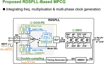
Summary: This paper presents a reference double-sampling phase-locked loop (RDSPLL)–based multi-phase clock generator (MPCG) that integrates frequency multiplication and octa-phase clock generation in a single system. Unlike conventional MPCGs relying on high-frequency global clocks, the proposed architecture directly generates high-frequency multi-phase clocks from a low-frequency reference, significantly reducing clock distribution power. Reference double sampling extends the loop bandwidth and enhances ring oscillator noise suppression, while an offset-compensated hybrid phase detector (OCH-PD) improves spur suppression and locking speed. Fabricated in 65-nm CMOS, the prototype achieves 674 fs jitter and −80 dBc reference spur with 3.43 mW, resulting in a FOMJitter-N of −251.9 dB.
IEEE Transactions on Circuits and Systems II: Express Briefs
Paper 1:
B. Ding, Y. Song; L. Dai; and S. Lin, “A 7-bit 76–81-GHz Hybrid Vector-Modulated Variable Gain Phase Shifter Combining Phase-Invariant VGA and 1-bit CDAC,” IEEE Transactions on Circuits and Systems II: Express Briefs, vol. 73, no. 1, pp. 28-32, Jan. 2026. doi: 10.1109/TCSII.2025.3635634
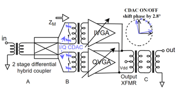
Summary: High-resolution phase shifters are essential for modern automotive radar beamforming, yet traditional designs face severe tradeoffs between resolution, bandwidth, and impedance stability. This work introduces a 77-GHz hybrid variable-gain phase shifter that combines a phase-invariant amplifier with a 1-bit capacitive DAC. By separating coarse and fine phase control, the proposed design achieves monotonic 7-bit phase resolution over a wide frequency range without calibration. Measurement results demonstrate stable gain, low phase error, and compact implementation. This approach offers a scalable and power-efficient solution for future high-performance mm-wave radar and phased-array systems.
Paper 2:
Y. Zhang, F. Huang, X. Tang, Z. Wei, Y. Cao, and Z. Li, “A Full-Band Reconfigurable CMOS Transceiver in the 50 MHz-to-7 GHz Frequency Range,” IEEE Transactions on Circuits and Systems II: Express Briefs, vol. 73, no. 1, pp. 48 - 52, Jan. 2026. doi: 10.1109/TCSII.2025.3629098
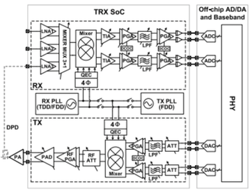
Summary: This work presents a full-band multi-mode reconfigurable CMOS transceiver (TRX) covering TDD/FDD 3GPP/WLAN, candidate 6G and WiFi 7 (5.925–7.125 GHz) frequency bands. A multi-mode architecture is proposed in the receiver (RX) chain, which supports reconfigurable low-noise (LN) and high-linearity (HL) operations with the RX chain reused for feedback observation (FBO). Powered by 1.2/2.5-V supplies, the 3.54×2.75 mm2 TRX circuit consumes 0.25 W/0.4 W in TDD/FDD modes. The present chip provides a fully reconfigurable solution for any carrier frequency from 50 MHz to 7 GHz with an instantaneous RF bandwidth of 110 MHz, with major performances comparable to the prior arts without resorting to digital calibration circuits.
Paper 3:
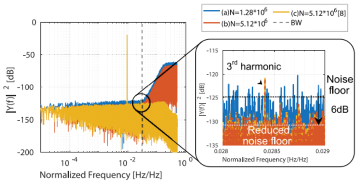
S. Ringeling, M. Fattori, R. Rutten, S. Bajoria, L. J. Breem, and E. Cantatore, “Cancellation of Quantization Noise in Sigma Delta Modulators Through Modeling of Non-Linearities,” IEEE Transactions on Circuits and Systems II: Express Briefs, vol. 72, no. 12, pp. 1862-1866, Dec. 2025. doi: 10.1109/TCSII.2025.3594847
Summary: IC design makes extensive use of circuit simulations to verify the chip performance before fabrication. One example of such a verification process is the linearity evaluation of Sigma Delta Modulators (SDM). Simulating circuit designs using general purpose commercial tools can be very time consuming, needing days to weeks for complex industrial designs. This work aims at reducing the required simulation time by applying suitable post-processing techniques, based on non-linear modelling of the SDM, to the existing circuit simulation. This post-processing technique lowers the quantization noise floor in the SDM frequency spectrum, without altering the linearity of the SDM, thus dramatically shortening the needed simulation time. The technique is demonstrated on a behavioural model of a 4th-order SDM with multiple sources of non-linearity, providing a 5000x simulation speedup, while keeping a very accurate linearity estimation.
IEEE Transactions on Circuits and Systems for Video Technologies
Paper 1:
Yimin Fu, Runqing Yang, Zhunga Liu, Michael K. Ng. "Adaptive Mixture-of-Experts Distillation for Cross-Satellite Generalizable Incremental Remote Sensing Scene Classification," IEEE Trans. on Circuits and Systems for Video Technology, vol.36, no.1, pp.233-247, Jan. 2026. doi: 10.1109/TCSVT.2025.359827.
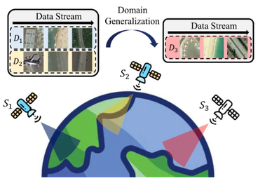
This paper proposes adaptive mixture-of-experts distillation (AMoED) for cross-satellite generalizable incremental remote sensing scene classification (CS-GIRSSC). Specifically, AMoED adopts a high-level semantic learning pipeline, in which new knowledge is acquired through the coordinated guidance of multiple domain-specific experts, rather than directly from raw data. This pipeline prevents the model from being exposed to large volumes of newly emerging data, thereby alleviating the erasure of previous knowledge when adapting to new data distributions. Besides, the adaptive mixture of domain-specific experts facilitates the formation of universal class concepts, which exhibit strong generalizability across different domains. During the learning process, an equi-partite subset is constructed for knowledge acquisition and consolidation, accompanied by a shallow style-mixing operation to mitigate the interference of domain discrepancies. Extensive experiments have been conducted on four remote sensing scene classification datasets, and the method proposed in this paper consistently shows state-of-the-art performance across various scenarios and settings. The code has been also made available by the authors at https://github.com/fuyimin96/AMoED
Paper 2:
Xiao Wang, Chao Wang, Shiao Wang, Xixi Wang, Zhicheng Zhao, Lin Zhu. "MambaEVT: Event Stream-Based Visual Object Tracking Using State Space Model," IEEE Trans. on Circuits and Systems for Video Technology, vol.36, no.1, pp.278-291, Jan. 2026. doi: 10.1109/TCSVT.2025.3588533.
This paper proposes a Mamba-based visual tracking framework that adopts the state space model with linear complexity as a backbone network. The search regions and target template are fed into the vision Mamba network for simultaneous feature extraction and interaction. The output tokens of search regions will be fed into the tracking head for target localization. More importantly, a dynamic template update strategy is introduced into the tracking framework using the Memory Mamba network. By considering the diversity of samples in the target template library and making appropriate adjustments to the template memory module, an effective dynamic template can be integrated. The effective combination of dynamic and static templates allows the proposed Mamba-based tracking algorithm to achieve a good balance between accuracy and computational cost on multiple large-scale datasets, including EventVOT, VisEvent, and FE240hz. The source code and checkpoint of this work have been released on https://github.com/Event-AHU/MambaEVT
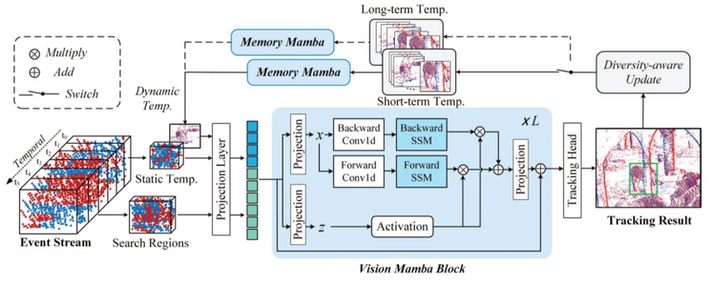
Overview of the proposed pure Mamba-based visual object tracking using an event camera, termed MambaEVT. The vision Mamba based backbone network performs feature extraction, interaction and fusion, simultaneously. It ensures the tracker achieves good performance and lowers computational cost. The learnable Memory Mamba for dynamic template generation makes the tracker more robust to significant appearance variation.
Paper 3:
Nian Wang, Zhigao Cui, Yanzhao Su, Yunwei Lan, Yuanliang Xue, Cong Zhang. "Weakly Supervised Image Dehazing via Physics-Based Decomposition," in IEEE Trans. on Circuits and Systems for Video Technology, vol.36, no.1, pp.637-652, Jan. 2026, doi: 10.1109/TCSVT.2025.3596024.
This paper proposes a weakly supervised image dehazing (WSID) model via physics-based decomposition (PBD). The proposed approach estimates atmospheric light, scattering coefficient and scene depth of real haze input to effectively capture the illumination information and haze distribution to recover a preliminary dehazed image by minimizing reconstruction loss. With this constraint, a subtly discrete wavelet discriminator (DWD) is designed to effectively improve the generalization to real scene from both spatial and frequency aspect under the supervision of unpaired real clear image. The PBD is a purely data-driven model freeing from any manual setting or partially correct prior, thus simultaneously ensuring the realness and visibility of dehazed images. Experiments on seven benchmarks have been reported in the paper showing the strong generalization ability of the proposed PBD, which achieves SOTA dehazing performance with realistic details. The code has been made available by the authors at the following link at https://github.com/NianWang-HJJGCDX/PBD
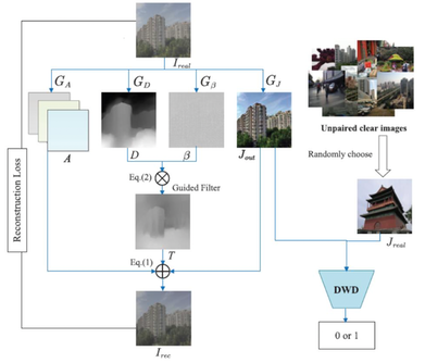
Workflow of the PBD proposed in this paper. First, four generators are used to yield the dehazed image Jout, scattering coefficient β, scene depth D, global atmospheric light A. The β and D capture the haze distribution of input real haze image Ireal and obtain a refined transmission map T. Reconstruction loss is used to constrain the structure information of these parameters. Then DWD improves the generalization ability of Jout and makes it fit in various real haze scenes via the adversarial training from both spatial and frequency aspect.
IEEE Transactions on Very Large Scale Integration (VLSI) Systems
Paper 1:
Das, S., Riedel, S., Naeim, M., Brunion, M., Bertuletti, M., Benini, L., Ryckaert, J., Myers, J., Biswas, D. and Milojevic, D., 2024. "Bandwidth-Latency-Thermal Co-Optimization of Interconnect-Dominated Many-Core 3D-IC," IEEE Transactions on Very Large Scale Integration (VLSI) Systems. vol. 33, no. 2, pp. 346-357, Feb. 2025, doi: 10.1109/TVLSI.2024.3467148 https://ieeexplore.ieee.org/document/10720515
Summary: The article addresses the challenges faced by contemporary system-on-chips (SoCs) due to the increasing demands for memory bandwidth, capacity, and thermal stability, particularly in the context of advancing artificial intelligence (AI). It proposes architectural modifications for a many-core SoC designed to enhance on-chip cache memory bandwidth and optimize access latency. The SoC is fabricated using A10 nanosheet technology in a 3-D configuration, with thermal analyses conducted. Workload simulations demonstrate significant performance improvements, achieving up to 12-fold acceleration for a 64-core version and 2.5-fold for a 16-core version, accompanied by a 40% increase in die area and a 60% rise in power dissipation when using a 2-D design. In comparison, the 3-D design not only minimizes the physical footprint but also saves 20% in power consumption due to a 40% reduction in wirelength. The study emphasizes the importance of restructuring pipelines to optimize the benefits of 3-D technology for enhanced memory access and lower latency. Additionally, it explores thermal impacts of different 3-D partitioning approaches in high-performance computing (HPC) and mobile applications, finding that 3-D designs in mobile contexts only slightly increase maximum temperature (by about 2-3 °C) compared to 2-D, while HPC scenarios require careful partitioning strategies to effectively manage thermal constraints.
Paper 2:
G. Murali, M. Gyu Park and S. Kyu Lim, "3DNN-Xplorer: A Machine Learning Framework for Design Space Exploration of Heterogeneous 3-D DNN Accelerators," IEEE Transactions on Very Large Scale Integration (VLSI) Systems, vol. 33, no. 2, pp. 358-370, Feb. 2025, doi: 10.1109/TVLSI.2024.3471496. https://ieeexplore.ieee.org/document/10715720
Summary: This paper introduces 3DNN-Xplorer, a novel machine learning (ML)-based framework for predicting the performance of heterogeneous 3-D deep neural network (DNN) accelerators. This framework enables design space exploration (DSE) of these accelerators with a two-tier compute-on-memory (CoM) configuration, considering 3-D physical design factors. The framework explores four distinct heterogeneous 3-D integration styles combining 28-nm and 16-nm technology nodes for both compute and memory tiers. Through extrapolation techniques and ML models trained on various accelerator configurations, the performance of larger systems is estimated, achieving a maximum absolute error of 13.9%. The framework considers area imbalance arising from different technology nodes by assuming equal numbers of PEs or on-chip memory capacity across integration styles. The analysis reveals that the heterogeneous 3-D style with 28-nm compute and 16-nm memory demonstrates energy-efficient performance, offering up to 50% energy savings and an 8.8% reduction in runtime compared to other 3-D integration styles. Conversely, the heterogeneous 3-D style with 16-nm compute and 28-nm memory proves area-efficient, exhibiting up to 8.3% runtime reduction compared to other 3-D styles.
Paper 3:
A. Almeida da Silva, L. Nogueira, A. Coelho, J. A. N. Silveira and C. Marcon, "Securet3d: An Adaptive, Secure, and Fault-Tolerant Aware Routing Algorithm for Vertically–Partially Connected 3D-NoC," IEEE Transactions on Very Large Scale Integration (VLSI) Systems, vol. 33, no. 1, pp. 275-287, Jan. 2025, doi: 10.1109/TVLSI.2024.3500575 https://ieeexplore.ieee.org/document/10766899
Summary: This article presents Securet3d, a novel routing algorithm designed for multiprocessor systems-on-chip (MPSoCs) that utilize 3-D networks-on-chip (3D-NoCs), aimed at enhancing secure and fault-tolerant operations. As MPSoCs play a crucial role in achieving effective parallel computing by sharing resources across complex applications, implementing adaptive mechanisms to safeguard sensitive data is essential. Securet3d builds upon the existing Reflect3d algorithm, introducing a comprehensive mapping scheme for secure data pathways and improving the system’s fault tolerance. The algorithm's effectiveness is validated through comparisons with three other fault-tolerant routing algorithms in vertically-partially connected 3D-NoCs. All algorithms were developed in SystemVerilog and evaluated via simulations using ModelSim, and hardware synthesis was performed with Cadence’s Genus tool. The experimental results indicate that Securet3d not only reduces latency but also enhances cost-effectiveness compared to other methods. Implemented with a 28-nm technology library, Securet3d exhibits minimal area and energy overhead, demonstrating its scalability and efficiency. Moreover, during denial-of-service (DoS) attacks, Securet3d maintains relatively stable average packet latencies of 70, 90, and 29 clock cycles for uniform random, bit-complement, and shuffle traffic, respectively, which are significantly lower than the latencies observed in other algorithms lacking security mechanisms (5763, 4632, and 3712 clock cycles on average). These findings underscore Securet3d's superior security, scalability, and adaptability for complex communication systems.
IEEE Journal on Emerging and Selected Topics in Circuits and Systems
Paper 1:
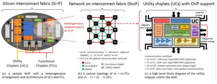
A. Delavari and B. Vaisband, "Chiplets Interface Protocol (ChIP) for Ultra-Large-Scale Applications," in IEEE Journal on Emerging and Selected Topics in Circuits and Systems, vol. 15, no. 4, pp. 585-598, Dec. 2025, doi: 10.1109/JETCAS.2025.3591559
Summary: As computational workloads continue to grow, heterogeneous integration of chiplet-based systems is becoming critically important for data-intensive applications such as highperformance computing, large language models, and artificial intelligence. Scaling to ultra-large systems introduces, however, significant communication challenges due to the limitations of network architectures and packaging technologies. Efficient data transfer across a network of thousands of chiplets remains a critical bottleneck. A robust, low-latency, area- and energy-efficient communication architecture for ultra-large-scale (ULS) system named Chiplet Interface Protocol (ChIP) is proposed in this work. ChIP supports burst transfers and out-of-order transactions while leveraging the simple universal parallel interface for chips (SuperCHIPS) - a simple area- and energy-efficient streaming channel at the physical layer. Evaluated on a wafer-scale platform, ChIP was compared to state-of-theart (SOTA) protocols, including LIPINCON, BoW, UCIe, and AIB, in performance, hardware efficiency, and unified signaling figures of merit. From the comparison results, ChIP significantly outperforms the SOTA alternatives (5.53X better) in bandwidth per shoreline, reaching 2.2 Tbps/mm in pipelined mode and up to 7.3 Tbps/mm in burst transactions. In addition, the transceiver area per link in ChIP is 485 μm^2 - 46.1% smaller than the best SOTA alternative - while achieving 0.38-0.53 pJ/bit energy and 1 ns latency in 45 nm CMOS over a 0.5 mm link, with efficiency sustained across longer channels and varied packaging due to minimal handshaking and optimized point-to-point specifications. The performance of ChIP is evaluated across multiple network configurations on a wafer-scale platform, and also for a customized hybrid topology, referred to as the network on interconnect fabric (NoIF), that is introduced and analyzed in this work. The architecture of the NoIF forms the foundation for ULS computing platforms, delivering exceptional results as compared to SOTA solutions. The superior hardware efficiency and advanced inter-chiplet communication features of ChIP position this proposed protocol as an ideal candidate for chiplet communication in ULS architectures. Learn more: https://ieeexplore.ieee.org/document/11088081
Paper 2:
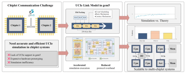
K. Li et al., "Efficient Die-to-Die Communication: UCIe Link Simulation and Optimization in a Chiplet-Based System," in IEEE Journal on Emerging and Selected Topics in Circuits and Systems, vol. 15, no. 4, pp. 599-608, Dec. 2025, doi: 10.1109/JETCAS.2025.3590822.
Summary: With the rapid advancement of chiplet-based architectures and heterogeneous computing platforms, accurate and high-fidelity interconnect modeling has become increasingly critical for early-stage architectural exploration and design evaluation. However, existing gem5 infrastructures do not provide native support for the Universal Chiplet Interconnect Express (UCIe) standard, compelling researchers to rely either on costly hardware prototyping or on simplified simulation models with limited representational accuracy. This paper presents a comprehensive system-level implementation of a UCIe link model within the gem5 simulation environment. The proposed framework integrates a flit-based packing mechanism compliant with the PCIe 6.0 256B flit mode, an Ack/Nak-based retry mechanism enhanced with a single-retry strategy for improved robustness, and an optimized event-driven scheduling scheme to substantially reduce simulation overhead. In addition, a parameterized latency modeling framework is introduced to facilitate precise calibration of configurable delay components in accordance with UCIe performance targets. Experimental evaluations demonstrate high modeling accuracy, with simulated link latency deviating by less than 0.5% from theoretical predictions. Compared with direct interconnects, the proposed UCIe model incurs less than 0.7% protocol overhead while maintaining scalability. The framework thus provides a high-precision, cost-effective virtual verification platform for future large-scale chiplet-based system design.
Paper 3:
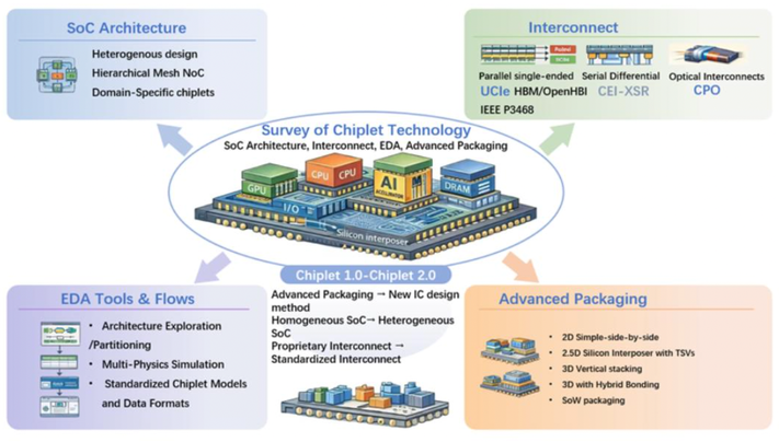
H. Liu et al., "Survey of Chiplet Technology: SoC Architecture, Interconnect, EDA, and Advanced Packaging," in IEEE Journal on Emerging and Selected Topics in Circuits and Systems, vol. 15, no. 4, pp. 514-536, Dec. 2025, doi: 10.1109/JETCAS.2025.3636408
Summary: Chiplet technology has emerged as a transformative approach in integrated circuit design. Although it has attracted significant attention recently, there has been limited effort dedicated to clearly defining its concept, terminology, composition, and evolution phases etc. This survey paper gives a formal definition by proposing chiplet terminology and composition, name it as a new design methodology, then analyze over 200 recent publications from both academia and industry to establish chiplet as a technology domain composed of four distinct fields: chiplet-based SoC architecture, interconnect, EDA tools, and advanced packaging. For each field composing chiplets, the paper traces the technology development, analyze challenges, outline the evolution trend and challenges. This survey aims to provides an in-depth examination of chiplet domain and each field’s progress, offering insights drawn from literature analysis to outline the current and emerging landscape of chiplet technology.
IEEE Open Journal of Circuits and Systems
Paper 1:
T. Kaiser, E. Gottschalk, K. Biethahn and F. Gerfers, "Pasithea-1: An Energy-Efficient Sequential Reconfigurable Array With CPU-Like Programmability," IEEE Open Journal of Circuits and Systems, vol. 6, pp. 1-13, 2025, doi: 10.1109/OJCAS.2024.3518110. https://ieeexplore.ieee.org/document/10802954
Summary: This work presents Pasithea-1, a coarse-grained reconfigurable array (CGRA) that combines energy efficiency with CPU-like programmability.
Paper 2:
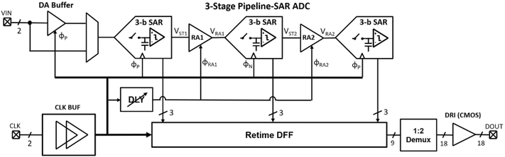
B. Yang, T. Caldwell and A. Chan Carusone, "An Energy-Efficient Pipeline-SAR ADC Using Linearized Dynamic Amplifiers and Input Buffer in 22nm FDSOI," IEEE Open Journal of Circuits and Systems, vol. 6, pp. 50-62, 2025, doi: 10.1109/OJCAS.2024.3509746. https://ieeexplore.ieee.org/document/10774063
Summary: This work presents a dynamic amplifier that achieves −52 dB in total harmonic distortion through an analog technique by which the expanding and compressing nonlinearities in the input transistors cancel one another. A pipeline-SAR analog-to-digital converter incorporating the linearized dynamic amplifier in both the input buffer and the first residue amplifier stage was designed and fabricated using the GlobalFoundries 22nm fully depleted silicon-on-insulator process.
Paper 3:
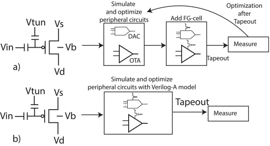
S. Nowshin Chowdhury, M. Chen and S. Shah, "Analysis and Verilog-A Modeling of Floating-Gate Transistors," IEEE Open Journal of Circuits and Systems, vol. 6, pp. 63-73, 2025, doi: 10.1109/OJCAS.2024.3524363. https://ieeexplore.ieee.org/document/10818976
Summary: This work presents a Verilog-A model based on empirical measurements for a floating-gate transistor fabricated using a 65 nm CMOS process.
________________
IEEE CAS Magazine Fourth Quarter Issue 2025
Now available: Fourth Quarter Issue

IEEE Circuits and Systems (CAS) Magazine publishes original review articles and other articles that are of broad interest to the Circuits and Systems Society community. Interested authors are invited to send a three to four page White Paper first to the Editor-in-Chief, Prof. Keshab K. Parhi, by email here. If invited, they can submit a Full Paper at the Author Portal at the link below. CAS Magazine will continue to publish articles related to CAS Society Outreach. In addition, CAS Magazine also publishes articles related to education (such as tricks in solving problems and short lecture notes), conference highlights, chapter highlights, applications, and standards. Please feel free to submit articles that are of broad interest to the members of the CAS Society. For more information, please visit the IEEE Circuits and Systems Magazine on the CASS website.
________________
Active "Call for Papers” Archive

______________________________
Latest Tables of Contents of CAS Sponsored Journals
The latest issues of our CAS sponored journals have been published and the tables of contents can be accessed through the following links:

- IEEE Transactions on Circuits and Systems I: Regular Papers
- IEEE Transactions on Circuits and Systems II: Express Briefs
- IEEE Transactions on Circuits and Systems for Video Technology
- IEEE Journal on Emerging and Selected Topics in Circuits and Systems
- IEEE Circuits and Systems Magazine
- IEEE Transactions on Biomedical Circuits and Systems
- IEEE Design and Test Magaz